| Q switch driver with Offset |
|
|
|
|
|
|
|
Some crystals used for pockels cell have significant peizzo
electric effects. When the voltage accross such a crystal is
changed quickly, strain can be induced in the material. Often
the strain will produce bifringence within the cell that counteracts
the bifringence being induced by the pockels effect. In pulsed
systems this effect is simply overcome by increasing the amplitude
of the applied pulse to greater than that required for DC induced
retardation. However, in simpler systems that just apply a voltage
and then remove it, the fast removal can result in strain and
the cell may not return to its quiescent state for some time,
related to acoustic time scales. To overcome this some Q switch
drivers offer the possibility to switch beyond ground, i.e. charge
to some voltage V and then switch down to -ΔV.
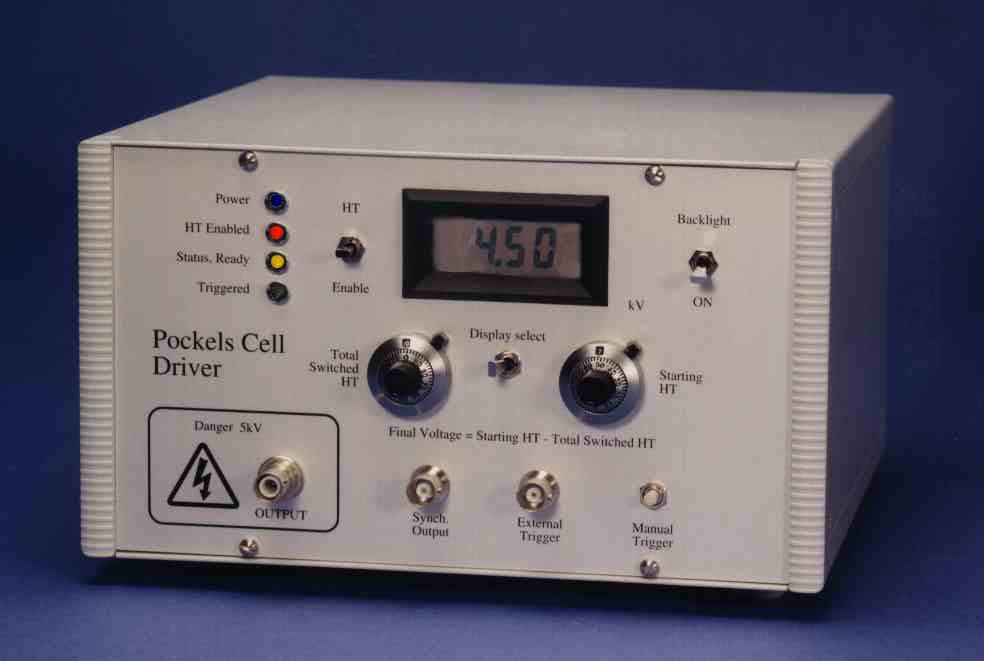
This new Q switch driver offers completely independent setting of the initial votage and the size of the voltage step applied to the cell. For example for simple piezzo electric effect compensation the output could be set at -2kV DC and then switched up by 2.5kV to 0.5kV. However, the output DC level can be set over a range at least equal to that of the switch so that at zero DC output the switch will take it to 2.5kV or at -4.5kV the switch will take it to -2kV. In principal one could bias the cell at V
λ/2 and then switch it to V
-λ/2. this would result
in transmission only over the transition time of around 5ns (depending
upon the load capacitance).
This product is currently available as a -4.5kV switch and -4.5kV bias but higher voltages are possible, certainly up to -8.5kV. Positive voltages can also be manufactured for applications that are polarity sensitive.